说明,这个是一个toshiba的nand flash(page size是512B+16B=528Byes)的datasheet中关于nand flash的page的read操作。解释的算是比较清楚。所以摘录下来以便大家看。感兴趣下载全文看:
NAND Flash Applications Design Guide from Toshiba (explains the low-level details of interfacing with common NAND flash chips)
3.1 Page Read
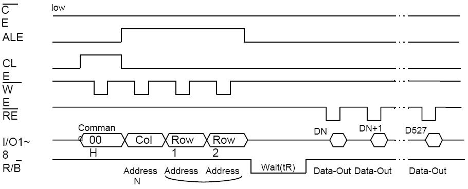
In a page read operation, a page of 528 bytes is transferred from memory into the data register for output. The sequence is as follows:
• Command phase: With CLE=1, ALE=0, the command byte 00h is placed on the I/O pins and WE# is brought low, then high. This stores the “read mode 1” command into the command register.
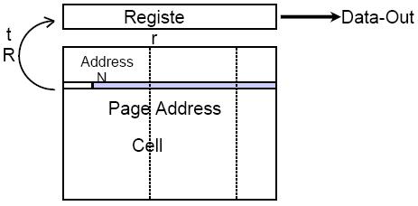
• Address phase: With CLE=0, ALE=1, the first address byte is placed on the I/O pins and WE# is toggled. This first address byte “N” (called the column byte in the figure below) is usually set to 0 in order to start reading from the beginning of the page. It is possible to set N to any value between 0 and 255. Because the page is actually 528 bytes long, a different read command is used if you want output data to start from byte 256-511 (read mode 2 – command byte 01h is used instead of 00h). A third read command is used if you want output data to come from bytes 512-527 (read mode 3 – command byte 50h is used instead of 00h). It should be noted that the full page is read from memory into the register. The value N, in conjunction with the read command used, simply sets the output data pointer within the register. The address bytes which follow after column byte N, indicated by Row1 and Row2 in the figure, are used to set the page within a block (lowest 5 bits in byte Row1), and the block within the device. In the higher density NAND devices, the address phase is 4 bytes long rather than 3.
• Data Transfer phase: CLE and ALE are set to zero while the chip goes busy in preparation for data readout. During the busy period, the ready/busy pin (R/B) goes low for up to 25 microseconds while data is being read from the memory array and transferred into the data register. During this period, it is important that chip enable is held low to keep the read operation from being stopped mid-cycle (note: this restriction is removed in a new family of NAND flash devices known as CE don’t care).
• Read Out phase: Once R/B returns high, data is available in the data register for read out. The first data byte output is byte N. Each RE# pulse reads out the next byte in the register. Once the last byte (D527) is read out, standard NAND flash will automatically go busy (another data transfer phase) in preparation for reading out the next page (with no additional command or address input). In the datasheet, this is called sequential read. If this is not desired, chip enable must be brought high (note: for the CE don’t care family of NAND flash, the automatic sequential read function does not exist).
Why is a page 528 bytes long? Since the original intent of the NAND flash was to replace magnetic hard disk drives, the intention was for the page to be big enough to store 1 sector (512 bytes) worth of data with 16 bytes extra for overhead such as error correcting code. Because the use of ECC is common with NAND flash (sample code is in the appendix), read mode 1 is the most often used read command because it enables one to read the entire 528 byte page.
转载请注明:在路上 » nand falsh read operation