关于nand flash 的 read disturb
最近在看资料,知道了一个nand flash的问题,叫做read disturb。
最准确的解释就是:
“Program Disturb: A program disturb error occurs when one or more bits not intended
to be programmed are changed from “1” to “0” during a PROGRAM operation. An
increased number of partial-page programs to a page can exacerbate this error. Program
disturb errors can show up on pages being programmed or on other pages within the
same block.
To recover from this type of error, erase the block where the error occurred and repro-
gram the data to that block.
Read Disturb: A read disturb error occurs when one or more bits are changed from “1”
to “0” during a READ operation. Read disturb errors occur within the block being read,
but on a page or pages other than the page being read. Performing a high number
(hundreds of thousands or millions) of READ operations on individual pages before an
ERASE command for the block containing those pages can exacerbate this error.
To recover from this type of error, erase the block where the error occurred and repro-
gram the data to that block.”
[PDF] TN-29-17: NAND Flash Design and Use Considerations
简单解释就是,你读取某个block内的某个page的数据的时候,结果,有时候会影响到此block内其他(相邻)的page里面的数据,从1变成0了。
具体原因,这个解释的相对清楚点:
先看这个解释:
“
So how does this read disturb work? Take a look at this drawing:
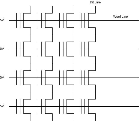
The drawing shows sixteen bit cells in a NAND Flash device. Each bit cell consists of nothing more than a MOSFET with a floating gate. To find out if there are any electrons trapped on a particular floating gate, the memory device must read out an entire word. It does this by putting a zero on the gates of all the bit cells in a word via the word line. However, because of the organization of the NAND Flash pages, the memory must also put some voltage on the gates of all the other MOSFETs in the block to turn on all of the other FETs in series in each bit line. NAND Flash memories are organized into strings of FETs to make them compact, small, cheap.
The high voltage on the MOSFETs’ gates attracts electrons to the floating gates, which is sort of like a write pulse, only shorter. Eventually, over time, some of those electrons will make it to the bit cell’s floating gate. When enough electrons make the jump, the cumulative read cycles will have caused a write and the data will be wrong. That’s the read-disturb problem. All NAND Flash parts have this problem and so the problem needs to be managed accordingly by periodically scrubbing each page in the NAND Flash memory.”
http://www.edn.com/blog/980000298/post/1670047767.html
再看这个解释:
“NAND-type flash memory exhibits the problems of read disturb and over-programming. In a read disturb, since a relatively high voltage is applied to non-selected word lines within a selected block (selected segments), memory cells, which are connected to non-selected word lines, assume a light programming operation state during a read operation. As a result of being subject to such field stress, the amount of charge within the floating gate increases, which in turn raises the memory cell threshold voltage. As a result, the threshold voltage of a memory cell in an erased state (data
http://www.freepatentsonline.com/6707714.html
上面的那些解释,我目前也没完全看懂,不过了解了大意:
由于内部单个某位数据,是如图一样,多个连在一起的,所以,对于某个位的读操作,而施加的高电压,使得电荷转移了,时间长了,积累到一定程度,就发生了真正的变化,再来一次读操作的时候,就相当于对旁边那些位进行write写操作了,导致数据从1变成了0,即read disturb现象。
此现象的解决办法就是前面提到过的,即擦出此block,也是这里说的:
“Recently our founder had lunch with a STMicro engineer that knew quite a bit about NAND and specifically the read-disturb failure modes. He told us that after 100,000 or so reads of a sector, the stored data is actually very likely to experience corruption. Subsequent reads of the sector will return the same corrupted data, but the flash sector can be erased and reprogrammed (with the same data or otherwise) for another 100,000 or so reads. Towards the end of the useable life of the flash, a written sector may only be good for 1000 (or less) reads before it looses value. He also reaffirmed that the quality of NAND chips have peaked and we should expect the NAND "quirks" to get worse in the future. ”
http://osdir.com/ml/file-systems.yaffs/2006-04/msg00037.html
转载请注明:在路上 » 关于nand flash 的 read disturb