Published in April/May 2006 issue of Chip Design Magazine
Flash Memory Moves from Niche to Mainstream
http://www.chipdesignmag.com/print.php?articleId=436?issueId=16
With the continuing growth of high-density NAND technologies, more embedded-Flash-drive devices are combining Flash media and a controller on a single chip.
With the massive deployment of high-speed data-transfer networks, users are being treated to an explosion of multimedia services. New devices are enabling services ranging from music phones, which are inspired by the success of MP3 players, to more general-purpose smart phones. The new multimedia-enabled handsets–and third-generation (3G) handsets in particular–have many common denominators. For instance, they all require much more memory. Users need to store both the content that they download from mobile network operators (MNOs) and their own personal data. The data may be private, such as photos and music. Or it may comprise professional e-mails and work documents. The memory in such handsets is therefore expected to reach densities of over 1 GB. Meanwhile, low-end 3G handsets will offer a bare minimum of 32 MB. Only a year ago, such requirements ranged from 16 to 256 MB.
Flash vendors have rallied to the call. They’re offering a range of high-density solutions that are based on various types of technologies, manufacturing processes, and form factors. Handset designers, for their part, are faced with the non-trivial task of sorting through all of these offerings and evaluating their benefits and tradeoffs. This effort requires a basic understanding of the differences between NOR, single-level-cell (SLC) NAND, and multi-level-cell (MLC) NAND Flash–the three major technologies in use. Designers also need a more in-depth understanding of how Flash vendors are implementing these technologies. The vendors’ goal is to enable handset OEMs to use them inside their newest models as quickly and cost effectively as possible.
FROM NOR TO NAND
The use of NAND-Flash technology in selected smart phones began in 2001 as an eyebrow-raising novelty. A mere handful of pioneering Flash vendors turned to NAND to meet seemingly contradictory memory requirements. They had to provide higher densities and better performance at lower costs and in smaller packages. Over the past two years, the number and proportion of NAND-based handsets has grown exponentially. Basic phones, which don’t require high-density memory, continue to use NOR Flash technology. But the deployment of 3G smart phones and high-end multimedia phones, which require both high-density embedded memory and high performance, has been largely responsible for the shift from NOR to NAND.
NAND-Flash revenues exceeded those of NOR Flash for the first time in the first quarter of 2005–only three years after NAND Flash was first introduced to mobile handset manufacturers in what was until then an exclusively NOR-Flash stronghold (Semico, May 2005). This dramatic success was the result of increased memory-card sales in growing densities. It also was driven by a massive penetration of NAND as an embedded nonvolatile-memory (NVM) solution.
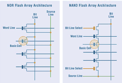
Figure 1: This figure compares the cell structures of NOR versus NAND devices.
The Table compares the key characteristics of the NOR and NAND technologies. NAND is ideal for high-density data storage, while NOR is best suited for use in code storage and execution–usually in low densities. Due to the efficient architecture of NAND Flash, its cell size is almost half the size of a NOR cell (see Figure 1). This characteristic, when combined with a simpler production process, enables NAND to offer higher densities with more memory on a given die size. The result is lower cost per MB.
NOR dominates the market in density ranges from 1 to 32 MB, while the sweet spot for NAND is 128 MB to 1 GB. (16 to 64 MB are available in small quantities and older processes.) These figures again stress the role of NOR devices for code storage and NAND devices for data storage–particularly for data-rich applications.
FROM SINGLE- TO MULTI-LEVEL-CELL NAND
NAND technology is constantly being improved to accommodate the growing demand for more embedded storage and higher performance at lower costs and in smaller packages. NAND Flash is evolving more quickly than the rate established by Moore’s Law. It is doubling in density every 12 months instead of every 18 months. This evolution is being achieved both by a smaller, more precise manufacturing process (down from 130 nm in 2003 to 90-70 nm in 2005) and altered physical characteristics. The page size, for instance, has jumped from 512 B to 2 KB. The block size has gone from 32 to 128 KB. In addition to enabling higher densities, the increase in page and block sizes enhances performance. It therefore provides acceptable response rates to store more data efficiently.
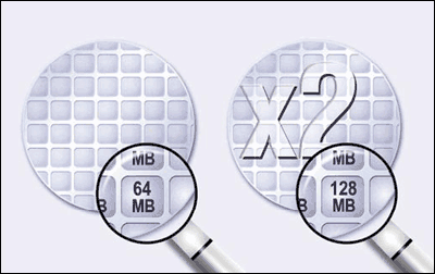
Figure 2: MLC NAND doubles Flash density in comparison to SLC NAND.
A major leap forward in NAND Flash was made with the introduction of multi-level-cell (MLC) NAND Flash in 2003. With single-level-cell (SLC) NAND, the standard 1 bit per cell was stored. In contrast, MLC NAND stores 2 bits per cell while increasing the density in a given die by up to 80% (see Figure 2). As a result, MLC NAND offers a superior cost structure. It comes with a penalty, however: Its performance and reliability are lower than SLC NAND. Despite this flaw, the performance of MLC NAND remains both significantly superior to NOR and in excess of multimedia handset requirements.
While MLC NAND represents a breakthrough in the cost structure, the technology’s inherent limitations make it difficult to integrate into real-life applications:
- Slower write performance: Though read performance is similar with SLC NAND, MLC NAND delivers slower write performance.
- Lower reliability: As noted previously, NAND Flash suffers from occasional bit flips. SLC NAND can have 1 bit error per page. MLC NAND, on the other hand, can have up to 4 bit errors per page and more in the future generations. These errors occur much more frequently in NAND Flash than they do in SLC NAND. In addition, MLC NAND has a much higher level of bad blocks (up to 5%), which in turn requires a more efficient management scheme.
- Incompatible Flash management: Even the basic functionality of MLC NAND is different from that of SLC NAND. Unlike SLC NAND, for example, MLC NAND must be accessed sequentially (i.e., once a block is accessed, its pages must be filled sequentially). With SLC NAND, free pages can be written in any order. Even if write operations to a particular page with MLC NAND are successful, adjacent pages may suffer from bit flips as a result of that write operation. Higher functionality further complicates the use of MLC NAND, making it necessary to implement more advanced, Flash-management algorithms and controllers.
FROM RAW NAND TO EMBEDDED FLASH DRIVES
When NAND was first introduced to the mobile handset market, its successful implementation depended on using an Embedded Flash Drive (EFD). EFDs integrate the Flash media along with a Flash controller on the same chip. They also include specially developed Flash-management software. The very first EFD was M-Systems’ DiskOnChip (also sold by Toshiba).
EFDs offer access to the NAND media through a legacy, NOR-like interface. They also provide an eXecute In Place (XIP) boot block, which makes it possible to completely remove the NOR Flash from the host system and thereby reduce the bill of materials (BOM). Additional features include more efficient power consumption, better performance, and security.
EFDs are becoming even more important as processes continually shrink, NAND-Flash qualities degrade, and the market share of complicated-to-use MLC NAND grows. EFDs deliver an easy and consistent way to implement the latest NAND technology. Memory designers aren’t required to be NAND experts. Nor are they forced to compromise on using older-generation NAND components supported by chip sets.
Today, most NAND-Flash manufacturers offer EFD solutions. This trend testifies to their acceptance and success in the multimedia handset market, where they meet ever-growing data storage requirements. The EFD solutions being offered today include M-Systems’ DiskOnChip, Renesas’ SuperAND, Sandisk’s iNAND, and Samsung’s OneNAND. Newcomers to the Flash industry are allegedly planning to introduce their own EFD solutions this year.
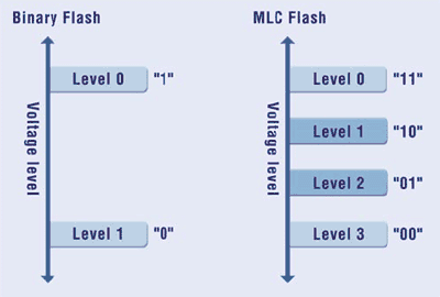
Figure 3: This comparison of different memory architectures shows the benefits of building Flash-management software into the controller as firmware.
FROM OLD TO NEW HURDLES
As NAND technology moves into mainstream and high-volume projects, the challenges for handset designers have changed. A few years ago, the issue of using NAND was mostly a technical one. No chip set supported NAND in 2001. The only way to design a NAND-based solution was by using an EFD. Today, most chip sets provide support for SLC NAND. Yet chip-set support for MLC NAND remains a challenge. In addition, two new hurdles have been spawned by the high demand for NAND technology driven by multimedia handsets and the Apple iPod nano: Flash allocation as demand exceeds supply and enabling access to the most advanced NAND technologies.
Handset vendors that use a multiple-source solution can minimize the impact of Flash allocation. In contrast, those using a single-source solution will be forced to pay higher prices. They also are likely to be allocated less supply than they need to meet customer demands. Aside from directly impacting their market share, this issue may lead to customer loss.
The issue of allocation is further complicated by the fact that advances in NAND-Flash technology and processes evolve much more rapidly than chip sets. Smart-phone chip sets, for instance, began supporting small-block SLC NAND Flash at the end of 2003. Earlier that year, both large-block SLC and MLC NAND had already been introduced. Large-block NAND was finally supported by a few chip sets by the end of 2005. Yet MLC NAND isn’t expected to have chip-set support until the end of this year. Despite NAND’s overwhelming acceptance in the handset market, the lower-end chip sets that target feature phones don’t yet offer any NAND support.
Instead of designing a new platform for each project, most customers design a particular platform for numerous projects. The lifespan of a platform is usually about two years. Designing a platform that supports the latest NAND technology is a complex process. The most critical and time-consuming task is to update the software running on the host in order to manage the Flash. This task requires intensive testing. In many cases, designers would rather delay access to new technologies until the next-generation platform.
If the Flash-management software doesn’t reside on the host, however, the integration process can be greatly simplified. New EFDs have successfully adopted this new approach. It enables them to be integrated as plug-and-play devices while using the most advanced and cost-effective NAND technologies. This new generation of EFDs offers an improved architecture: The Flash-management software is built into the controller as firmware, rather than being coupled with the host (see Figure 3). Offering an easy block-device interface minimizes the design effort for handset vendors. They can then move to the next NAND technology without changing the host design.
As the mobile market continues to offer more and increasingly sophisticated multimedia applications, the need for memory is exponentially increasing. This need is justifying the move from NOR-based to NAND-based handsets. To answer these market challenges–both technical and business–handset manufacturers would be wise to implement complete, advanced memory solutions like second-generation EFDs. By comparison, Flash components would require heavier integration efforts and higher design costs.
As NAND Flash gains industry acceptance as the best technology for today’s high-density data storage, application processors are just beginning to support NAND interfaces. As the fast pace of advanced, higher-density NAND technologies continues into the foreseeable future, second-generation EFDs will have considerable added value over raw NAND media. They’ll enable savvy handset manufacturers to cost effectively support new NAND technologies with plug-and-play integration ease. As a result, the manufacturers will get their new, high-density handset models to market faster.
Francois Kaplan, AVP Product Marketing for M-Systems’ mobile division, manages worldwide product marketing activities for both customers and partners. He earned an engineering degree from a top school in France, Ecole Centrale de Lyon. Mr. Kaplan can be reached at [email protected].