Flash memory – Principles of operation
Flash memory stores information in an array of floating gate transistors, called "cells", each of which traditionally stores one bit of information. Newer flash memory devices, sometimes referred to as multi-level cell devices, can store more than 1 bit per cell, by varying the number of electrons placed on the floating gate of a cell.
In NOR flash, each cell looks similar to a standard MOSFET transistor, except that it has two gates instead of just one. One gate is the control gate (CG) like in other MOS transistors, but the second is a floating gate (FG) that is insulated all around by an oxide layer. The FG is between the CG and the substrate. Because the FG is isolated by its insulating oxide layer, any electrons placed on it get trapped there and thus store the information. When electrons are on the FG, they modify (partially cancel out) the electric field coming from the CG, which modifies the threshold voltage (Vt) of the cell. Thus, when the cell is "read" by placing a specific voltage on the CG, electrical current will either flow or not flow, depending on the Vt of the cell, which is controlled by the number of electrons on the FG. This presence or absence of current is sensed and translated into 1’s and 0’s, reproducing the stored data. In a multi-level cell device, which stores more than 1 bit of information per cell, the amount of current flow will be sensed, rather than simply detecting presence or absence of current, in order to determine the number of electrons stored on the FG.
A NOR flash cell is programmed (set to a specified data value) by starting up electrons flowing from the source to the drain, then a large voltage placed on the CG provides a strong enough electric field to suck them up onto the FG, a process called hot-electron injection. To erase (reset to all 1’s, in preparation for reprogramming) a NOR flash cell, a large voltage differential is placed between the CG and source, which pulls the electrons off through quantum tunneling. In single-voltage devices (virtually all chips available today), this high voltage is generated by an on-chip charge pump. Most modern NOR flash memory components are divided into erase segments, usually called either blocks or sectors. All of the memory cells in a block must be erased at the same time. NOR programming, however, can generally be performed one byte or word at a time.
NAND Flash uses tunnel injection for writing and tunnel release for erasing. NAND flash memory forms the core of the removable USB interface storage devices known as keydrives.
principle of Flash Memory– SLC+MLC
Flash Memory is a semiconductor memory device that is electrically erasable and programmable in sections of memory called ‘blocks’. In a flash memory, a whole block of memory cells can be erased in a single action, or in a ‘flash,’ which is how this device got its name. Flash memory is non-volatile, i.e., it can retain its memory contents even if it is powered off.
A basic flash memory cell consists of a MOSFET that was modified to include an isolated inner gate between its external gate and the silicon (see Figure 1). This inner gate is known as a ‘floating gate’, which is the data-storing element of the memory cell. Flash memory is not the first memory device to use a floating gate to store information. The uv-erasable EPROM, which preceded the Flash memory, is also a ‘floating gate’ memory device.
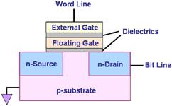
Figure 1. A Typical Flash Memory Cell
Data is stored in a flash memory cell in the form of electrical charge accumulated inside the floating gate. The amount of charge stored in the floating gate depends on the voltage applied to the external gate of the memory cell that controls the flow of charge into or out of the floating gate. The data contained in the cell depends on whether the voltage of the stored charge exceeds a specified threshold voltage Vth or not.
Intel has developed flash memory technology wherein memory cells can hold two or more bits of data instead of just one each. The trick is to take advantage of the analog nature of the charge stored in the memory cell and allow it to charge to several different voltage levels. Each voltage range to which the floating gate can charge can then be assigned its own digital code. Thus, a 2-bit cell can distinguish 4 distinct voltage ranges, while a 3-bit one can distinguish 8 of them. Intel calls this technology ‘Multi-Level Cell (MLC)" technology.
A typical MLC consists of a single transistor with direct electrical connections to its gate, source, and drain that allow very precise control of the charging of the cell’s floating gate. For a multi-level cell to work, it must be able to deposit charge with precision, sense charge with precision, and store charge over time. High-precision charging and charge sensing are the key to a MLC’s ability to distinguish several charge levels. Table 1 illustrates how a 2-bit multi-level cell assigns digital codes to 4 different charge voltage levels.
Table 1. 2-Bit Intel MLC Digital Code Assignment
Charge Level | Digital Code |
Level 3 | 00 |
Level 2 | 01 |
Level 1 | 10 |
Level 0 | 11 |
MLC programming is accomplished by charging the floating gate through a precise process of Channel Hot-Electron (CHE) injection. During programming, the source of the MLC transistor is usually grounded. Column decoding of the MLC provides direct bitline connection to the drain which is pulsed at a constant voltage. Row decoding of the MLC, on the other hand, provides direct wordline connection that causes the MLC transistor gate to be connected to an internally generated supply voltage. This direct and precise control of the drain and gate is critical to the correct charging of the floating gate and, hence, correct storage of information.
Reading the contents of multi-level cells involves highly precise sensing of the amount of charge in the floating gate, measured in terms of cell currents that have an inverse relationship with the Vth. The sensed currents are compared to reference currents, with the comparison results inputted to a logic circuit that encodes them into the corresponding digital data.
Samsung SLC Flash Vs MLC Flash [Kingston Toshiba Hynix] Comparison
For all Flash Cards MERCURY is using Samsung Flash Chips and its Wafer is SLC. (Single Level Cell)
The newest MERCURY 1GB MMCmobile is also build with SLC Flash Chips.
For most Flash Cards Kingston is using Toshiba Flash Chips and its Wafer is MLC. The Kingston 1GB MMCmobile is build with MLC Flash Chips.(Multi Level Cell)
SLC Advantage
[What is SLC or MLC?]
Basically there are two different types of NAND flash.
The first is called SLC or single level cell flash while the second one is called MLC or multi level cell flash.
The main difference is that SLC stores a single bit of data per cell whereas MLC, by using a larger number of voltage levels, stores two bits of data per cell.
[What are the advantages of SLC?]
Unfortunately for the MLC flash, the ability to store more data per cell also came with reliability and performance disadvantages.
-Significantly slower read and write speeds.
-10x lower read/write lifetime (100,000 R/W -> SLC, 10,000 R/W -> MLC)
-Shorter data retention time.
-Thus SLC flash has much better performance, lifetime, and reliability properties than MLC.
[Conclusion]
MLC is used to reduce the cost for flash memory card production and is found in the majority of the lower speed generic cards.
SLC flash is used for higher performance flash memory and is only used by a few of the higher end flash card producers.
All MERCURY Flash cards use Samsung SLC NAND flash for maximum performance, reliability, and lifetime.
Engineers need to know the tradeoffs of NOR vs. NAND, and SLC vs. MLC
BY BRIAN KUMAGAI and SCOTT BEEKMAN
Toshiba America Electronic Components
Irvine, CA
http://www.toshiba.com/taec
Flash memory has become one of the fastest growing semiconductor memories because of widespread adoption of this nonvolatile memory in portable electronics devices and consumer applications. Two major types, NOR flash and NAND flash have become dominant in the market. NOR flash is often used in portable electronics devices, and it has been the leading memory architecture in cell phones and PDAs for code storage and direct execution.
Stacking techniques offer combinations of up to four different types of memory in a single BGA package.
NAND flash, which was designed with a very small cell size to enable a low cost per bit, is widely used as a high-density file storage medium for consumer devices such as digital cameras and MP3 players. This memory architecture is also becoming widely adopted for data storage in camera cell phones.
Today, the distinction between NAND and NOR has become blurry as new controller options make NAND an alternative for a wider range of applications. As the density of NAND flash has continued to increase and the cost per bit has decreased, memory subsystem designers in portable electronics now consider NAND for use in some traditional NOR applications to take advantage of its significantly faster write/erase performance.
Another factor to consider when selecting flash memory is the differences between single-level cell (SLC) flash and multilevel cell (MLC) flash. MLC NAND increases density in less silicon area by storing 2 bits per memory cell.
MLC technology has been applied to both NOR and NAND flash devices and has proven to be very cost effective for many applications. It also expands the range of performance characteristics, enabling design engineers to select the product that best matches the requirements of their system.
Designers may also want to consider memory subsystems that utilize both NOR and NAND flash. Tradeoffs in density, speed, cost and power make different types of memory desirable in many applications.
Today, multichip packages (MCP) that combine NOR, NAND, SRAM, SDRAM, and Pseudo SRAM to create memory subsystems in a single component are widely used in cellular phones, and may help designers of other electronic devices address the design challenge to provide higher-density higher-performance memory at a lower cost and in a smaller space. The following guidelines assess the tradeoffs in each area when selecting flash memory.
NOR vs. NAND
The characteristics of NOR flash are lower density, high read speed, slow write speed, slow erase speed, and a random-access interface. NOR flash is ideal for directly executing code such as boot or application code because its direct random-access interface allows a microprocessor to directly access any address location similar to a mask ROM or SRAM. The disadvantage of a random-access interface is the need to accommodate additional address lines when upgrading to a higher-density memory chip.
The characteristics of NAND flash are high density, medium read speed, high write speed, high erase speed, and an indirect or I/O like access. The indirect interface requires that the NAND flash must be accessed through a command sequence instead of through the direct application of an address to the address lines.
The NAND flash has internal command, address, and data registers. Although this interface may appear more cumbersome than the direct interface of NOR flash, a notable advantage is the relative ease in upgrading to a higher-density device.
Because of the indirect interface, the external pinout, or connection to the host, does not change with the density of the chip. This is similar to the hard-disk drive interface in which different densities of hard disk drives could use the same cable interface.
If there is a need to boot out of flash, execute code from the flash, or if read latency is an issue, NOR flash is better suited. However for storage applications, NAND flash’s higher density as well as its high programming and erase speeds make it the best choice.
While the benefit of high programming speed in high-density flash devices is obvious, erase performance is equally important, though less obvious. Unlike magnetic memory systems (hard-disk drives and tape drives), the programming of NAND flash only turns memory cells from the "1" state to the "0" state.
A separate erasing step is required to turn all bits back to the "1" state before the device is reprogrammed. In the table, the rewrite speed is the effective speed of both erasing and programming combined.
Multilevel flash
MLC NAND flash allows each memory cell to store 2 bits of information, compared to 1 bit-per-cell for SLC NAND flash, resulting in a larger capacity and lower bit cost. While SLC NAND may be more appropriate for some specific applications, the difference in performance will not affect many common consumer applications, including most digital camera uses.
MLC NAND provides a very competitive level of performance and makes high-density NAND cards more affordable, resulting in its growing popularity among consumers. For the current state of the art, the highest-density commercially available MLC NAND flash is 4 Gbits, whereas the highest-density MLC NOR flash is 256 Mbits.
As a rule of thumb, MLC devices are available at twice the density of SLC devices of the same flash technology. Mature and proven, MLC technology is generally used in cost-sensitive consumer products such as cell phones and memory cards.
A significant portion of the NAND flash-based memory cards on the market today are made from MLC NAND, and the continuing rapid growth of this market can be considered an indication that the performance is meeting consumers’ needs. Although the use of MLC technology offers the highest density (and the lowest cost), the tradeoff compared to single-bit-per cell is lower performance in the form of slower write (and potentially erase) speeds, as well as reduced write/erase cycling endurance.
Also, because of the storage of 2 bits per cell, the probability of bit error will be higher than for SLC technology. However, this is easily compensated for by using error detection and correction codes (EDC). System designers have long been aware of the benefits of using EDC to detect and correct errors in systems using Hamming codes (common in memory subsystems) and Reed Solomon codes (common in hard drives and CD-ROMs).
Cycle life
Currently, life expectancy of SLC flash is rated at approximately 100,000 cycles and MLC flash is rated to have approximately 10,000 cycles. In many cases, 10,000 erase cycles is more than sufficient.
For example, a 4-Mpixel digital camera’s 256MB MLC card can typically store around 250 pictures (a conservative estimate). Its 10,000 read/write cycles, combined with wear-leveling algorithms in the controller, will enable the user to store and/or view approximately 2.5 million pictures within the expected useful life of the card.
That number is so far beyond the average number of photos taken by the typical user that the difference in endurance is not significant for this application. In other cases, where high reliability, endurance, and performance are required, SLC flash is an appropriate choice.
Multichip packages
For applications that require code storage as well as high-density file storage, it may be a better solution to use both NOR and NAND, possibly with other types of memory. Multichip packages today are available to combine a complete, complex memory subsystem in a single, small package.
These devices have become widely used in cellular phones with added applications such as cameras and Internet browsers. Other portable devices might benefit from this approach.
For example, a BGA package with five stacked memory chips can be as small as 9 x 12 x 1.4 mm, depending on the specific memory configuration. Today, semicustom combinations of two, three, or four different types of memory, with stacks involving up to nine layers are being combined in a single package, with higher stacks on the horizon.
The conventional memory architecture for today’s multifunction cellular phones typically uses NOR flash for code storage, Pseudo SRAM for workspace, NAND flash for data storage, and�in some markets�SRAM for backup. Engineers can now balance the benefits of NOR vs. NAND, and SLC vs. MLC to best meet the needs of their design.
Flash memory erasure is achieved by ‘discharging’ the floating gate through a phenomenon known as Fowler-Nordheim tunneling, wherein electrons from the floating gate pass through the thin dielectric layer and get dissipated at the source of the memory cell transistor.
Flash memory is used in a variety of applications such as: personal and notebook computers, digital cell phones, digital cameras, portable memory devices, LAN switches, embedded controllers, etc.